


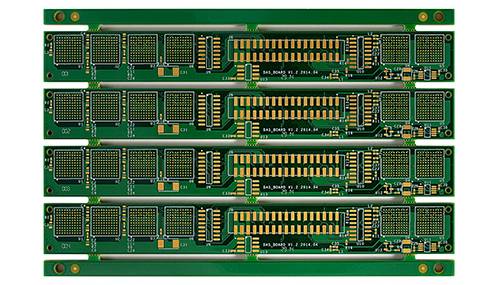
What Is HDI PCB Manufacturing?
High-Density Interconnect (HDI) PCB manufacturing involves creating printed circuit boards with finer lines, smaller vias, and higher wiring density than standard PCBs.
These advanced boards allow components to be packed closely, improving performance and reducing board size.
HDI PCBs typically use microvias, blind and buried vias, and sequential lamination to interconnect multiple layers efficiently.
Their compact architecture supports high-speed signal transmission and reduces crosstalk — making them essential for modern electronics such as smartphones, laptops, and automotive systems.
Manufacturers rely on precise laser drilling and advanced imaging to achieve fine features.
This process enables higher layer counts without increasing board thickness, maintaining strength and conductivity.
In short, HDI PCBs allow more functionality within smaller, lighter devices — a key factor in today’s compact, high-performance electronics.
Key Features of HDI PCBs
HDI boards stand out for their precision and density.
Key characteristics include:
-
Microvias: Extremely small holes connecting layers, improving signal quality.
-
High Layer Density: More interconnections per square inch.
-
Sequential Lamination: Layer-by-layer buildup for stability and strength.
-
Thin Dielectrics: Reduced signal loss and shorter transmission paths.
These features collectively enhance device performance while maintaining mechanical reliability.
Difference Between HDI and Standard PCBs
Standard PCBs use through-holes and larger trace widths, limiting component density.
HDI PCBs use microvias and advanced lamination to fit more components in less space.
HDI designs also allow shorter signal paths, reducing delay and improving signal quality.
As a result, they are more expensive but provide better performance for high-speed and miniaturized devices.
The HDI PCB Manufacturing Process
HDI manufacturing combines precision drilling, sequential lamination, and microvia plating.
Each step must meet strict tolerances to ensure consistent performance and durability.
Step 1 – Layer Stack-Up Design
The design phase determines the number of layers, materials, and via structures.
Engineers select high-Tg laminates and copper foils suitable for fine features.
Proper layer arrangement ensures balanced impedance and signal integrity.
Step 2 – Laser Drilling and Microvia Formation
Laser drilling creates microvias as small as 0.1mm.
This step replaces traditional mechanical drilling for better precision.
Microvias form interconnections between layers without affecting board stability.
Step 3 – Copper Plating and Via Filling
Once vias are drilled, they’re plated with copper to establish conductive pathways.
Filling techniques prevent voids, improving electrical reliability and heat dissipation.
Uniform plating is critical for performance consistency across layers.
Step 4 – Lamination and Etching
Each layer is laminated under heat and pressure to bond them into a single unit.
After lamination, copper etching defines circuit patterns and traces.
Inspection follows to ensure alignment and connectivity before final finishing.
Benefits of HDI PCB Technology
HDI technology enhances both electrical and mechanical performance.
Its precise interconnections and reduced parasitic effects make it ideal for advanced applications.
Compact Design and High Functionality
HDI boards enable tighter component spacing, allowing for miniaturized designs.
Despite their size, they support more complex circuits with faster signal transmission.
This makes them essential in smartphones, tablets, and aerospace systems.
Enhanced Signal Integrity and Reliability
Shorter paths reduce signal delay, noise, and electromagnetic interference.
Microvias provide stable electrical connections, minimizing failure risks.
These factors make HDI PCBs reliable for high-frequency, data-heavy devices.
Common Applications of HDI PCBs
HDI PCBs are widely used in industries demanding compact, high-speed performance:
-
Smartphones and wearable electronics
-
Medical imaging and diagnostic devices
-
Automotive radar and control systems
-
Aerospace and defense communication equipment
-
High-speed computing and networking hardware
Their balance of power, size, and precision makes them critical for innovation across multiple sectors.
Challenges and Cost Factors in HDI PCB Manufacturing
HDI PCBs require advanced materials, precision equipment, and skilled engineering.
This complexity increases production costs and turnaround times.
Factors affecting cost include:
-
Number of sequential laminations
-
Microvia count and size
-
Material type (e.g., high-Tg or low-Dk laminates)
-
Surface finish and plating requirements
Despite higher costs, HDI technology delivers unmatched electrical performance and reliability — justifying investment for high-end electronics.
Final Thoughts on HDI PCB Production
HDI PCB manufacturing represents the future of compact, high-speed electronics.
By combining advanced microvia design, multilayer integration, and precise fabrication, these boards deliver exceptional performance within limited space.
As technology evolves, HDI PCBs will remain a cornerstone in next-generation electronic design — driving innovation across communication, computing, and industrial sectors.

