


Creating your own printed circuit board (PCB) at home may sound like a project for engineers and electronics geeks, but thanks to readily available tools and materials, DIY PCB fabrication is easier than ever. Whether you’re a hobbyist, student, or professional looking to prototype your next big idea, learning how to make a printed circuit board at home is an essential and rewarding skill.
Table of Contents
ToggleIn this comprehensive PCB making tutorial, we’ll guide you through the entire process—from PCB design and making to homemade PCB etching. We’ll also share the best low-cost PCB production methods, safety tips, and even DIY PCB milling machine alternatives.
Let’s dive into the simplest and safest way to print your own circuit board at home.
What is a Printed Circuit Board (PCB)?
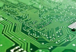
A printed circuit board (PCB) is the foundational building block of modern electronics. It mechanically supports and electrically connects components using conductive pathways etched from copper sheets laminated onto a non-conductive substrate.
When you print your own circuit board, you’re essentially creating a custom layout that allows electronic components to interact exactly how you need them to.
DIY PCB Fabrication – Overview of Methods
There are several popular methods for making PCBs at home safely. The two most common are:
- Toner Transfer Method (Easiest)
- Photoresist Method (More Precise)
- DIY PCB Milling Machine (Advanced)
We’ll focus on the toner transfer method because it offers the easiest way to make a printed circuit board at home with minimal tools and investment.
Step-by-Step Guide: How to Make a Printed Circuit Board at Home
This homemade circuit board steps guide uses the toner transfer method—perfect for beginners and ideal for PCB prototyping at home.
1. Design Your PCB Layout
Before anything else, you’ll need to design your PCB using software like:
- KiCad (Free & Open Source)
- Eagle
- Fritzing
- EasyEDA (Web-based)
These platforms allow you to create your schematic and convert it into a PCB layout. Once done, export your design as a PDF or Gerber file.
2. Print the PCB Layout
Keyword: print your own circuit board
- Print the layout on glossy paper or photo paper using a laser printer (not an inkjet).
- Ensure the toner side is printed in mirror format, so it aligns properly when transferred to the copper board.
Pro Tip: Print in high contrast black to ensure accurate toner transfer.
3. Prepare the Copper-Clad Board
- Cut your copper-clad board to match your PCB size.
- Clean the surface with fine sandpaper or steel wool to remove oxidation.
- Wash it with isopropyl alcohol to ensure oil-free contact.
4. Transfer the Toner to the Copper Board
Place the printed layout toner side down onto the copper board.
- Use a hot iron or laminator to apply heat and pressure.
- Heat for 3–5 minutes in circular motions.
- Let the board cool, then soak in warm water to remove the paper gently.
This step is crucial in low-cost PCB production as it ensures accuracy without specialized equipment.
5. Etch the PCB
Keyword: homemade PCB etching, pcb etching solution recipes
You’ll need a DIY etching solution. Here are some proven PCB etching solution recipes:
Common Ferric Chloride Recipe:
- Purchase ready-made Ferric Chloride (available online or electronics stores).
- Pour enough to submerge the board in a plastic container (never metal).
Alternative: Hydrogen Peroxide + Hydrochloric Acid
- 2 parts Hydrogen Peroxide (3%)
- 1 part Hydrochloric Acid (Muriatic Acid)
Use extreme caution and always wear gloves, goggles, and a respirator.
Agitate gently every minute. The exposed copper will dissolve, leaving only the traces.
6. Clean the Board
After etching, rinse with water. Use acetone or nail polish remover to remove the toner.
You’ll now see clean copper traces forming your circuit. Your homemade circuit board steps are almost complete.
7. Drill Component Holes
Use a 0.8–1mm drill bit and a PCB mini-drill to drill holes for your through-hole components.
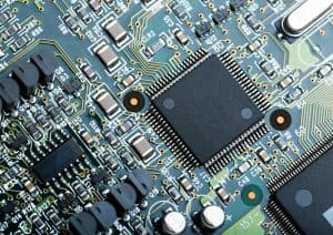
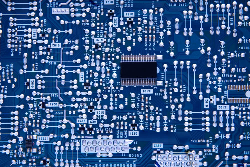
8. Solder the Components
Now it’s time to place and solder your components. Follow your schematic carefully and double-check the polarity for components like diodes, LEDs, and ICs.
Optional: Silkscreen and Solder Mask
While not essential, you can add labels (silkscreen) and a solder mask using UV-curable ink and transparencies, or use DIY PCB milling machines for more advanced fabrication.
Safety Tips for Making PCBs at Home
Keyword: making pcbs at home safely
- Ventilation: Always etch in a well-ventilated space.
- Gloves and Goggles: Use PPE to prevent chemical burns.
- Disposal: Dispose of chemicals responsibly. Contact local e-waste centers for guidance.
- Storage: Keep acids and solvents away from children and pets.
DIY PCB Milling Machine – When to Consider It
For precision and reusability, consider a CNC-based PCB milling machine. It removes copper to form traces rather than etching. Though the investment is higher, it’s excellent for rapid prototyping.
Popular DIY machines:
- Genmitsu CNC 3018-PRO
- EleksMaker A3 Pro
- OpenBuilds MiniMill
They work with Gerber files, and software like FlatCAM helps convert designs to millable paths.
Advantages of Homemade PCBs
- Customization: Tailor the board for any project.
- Cost Savings: Great for low-cost PCB production.
- Quick Turnaround: No need to wait for shipping.
- Learning Experience: Understand electronics at a deeper level.
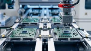
When to Use Professional PCB Fabrication Services?
While DIY is great, professional manufacturing (like at MKTPCB) is better when:
- Batch production is needed
- Multilayer boards are required
- High-frequency signals demand tighter tolerances
- SMD (Surface Mount Devices) assembly is involved
MKTPCB offers affordable, high-quality solutions tailored for prototyping and production alike.
Frequently Asked Questions (FAQs)
1. Is it safe to make PCBs at home?
Yes, if done responsibly. Use PPE like gloves and goggles, ensure good ventilation, and handle chemicals with care. Always follow making PCBs at home safely guidelines.
2. What’s the best method to etch a PCB?
The ferric chloride method is the most beginner-friendly. For better control, use the hydrogen peroxide + hydrochloric acid mix. For zero chemicals, try DIY PCB milling machines.
3. Can I print PCB designs at home without special equipment?
Yes. You can print your own circuit board using a laser printer and glossy paper. With an iron or laminator, you can transfer the design to the copper board easily.
4. What tools are essential for DIY PCB fabrication?
- Laser printer
- Glossy or photo paper
- Copper-clad board
- Clothes iron or laminator
- Etching solution
- Safety gear (gloves, goggles)
- PCB drill
- Soldering iron
5.How precise can homemade PCBs be?
With care, you can achieve 0.3mm trace widths, sufficient for most hobby projects. For ultra-fine traces or double-layer boards, professional manufacturing is recommended.
Final Thoughts
Learning how to make a printed circuit board at home opens up a world of creativity and innovation. From prototyping gadgets to fixing electronics, mastering DIY PCB fabrication gives you full control over your projects.
However, for advanced requirements or professional-grade PCBs, platforms like MKTPCB provide efficient, scalable, and affordable solutions with exceptional precision.
So, whether you’re making your first simple board or gearing up for production, you’re now equipped with the knowledge to take your electronics game to the next level.

