


Printed circuit board (PCB) gold fingers are essential for reliable edge connections.
They link PCBs to external devices through connectors and ensure minimal resistance.
This guide explains their design, standards, and benefits.
It serves engineers, students, and procurement teams seeking clear, actionable information.
By the end, readers will know how to design compliant and efficient PCB gold fingers.
What Are PCB Gold Fingers?
PCB gold fingers are the gold-plated contacts located along a PCB’s edge.
They function as the interface between the board and a connector.
These contacts are shaped like “fingers” for easy insertion and removal.
They’re coated with hard gold, an alloy of gold and cobalt or nickel, to improve durability.

Gold fingers handle power, signal, and data transmission.
Their thickness and length vary depending on the current or signal they must carry.
Common plating thicknesses range from 30 microinches to 50 microinches.
This thickness ensures consistent conductivity and wear resistance over repeated insertions.
Most high-speed communication boards, industrial control systems, and memory modules use gold fingers.
The feature reduces oxidation, ensuring a long-lasting and stable connection.
Unlike tin or copper contacts, gold provides low contact resistance even under harsh conditions.
In practice, PCB designers create gold fingers on the outermost layer.
They specify precise widths and spacing following connector specifications.
Later, the PCB manufacturer plates the contacts with nickel and then gold.
Knowing the purpose of gold fingers helps you plan for proper layout and cost.
It also sets the stage for meeting industry standards and achieving dependable performance.
Why Gold Fingers Matter in PCB Design
Gold fingers ensure signal integrity and mechanical reliability in edge connectors.
Without them, contact points wear quickly and corrode, leading to failures.
In high-frequency circuits, gold fingers reduce signal loss at the connection point.
They maintain low impedance paths for high-speed data.
This is critical in applications like servers, telecommunications, and aerospace systems.
Gold plating also resists corrosion from humidity and air pollutants.
This is especially valuable in industrial or outdoor environments.
By specifying gold fingers, designers extend the lifespan of their products.
Another key advantage is repeated mating cycles.
A typical PCB with tin contacts may degrade after a few hundred insertions.
Gold fingers can handle thousands of cycles while keeping stable resistance.
In addition, using standardized gold finger dimensions allows easy compatibility with off-the-shelf connectors.
This simplifies manufacturing and maintenance.
Thus, gold fingers are not a luxury feature.
They are a core part of robust, reliable PCB design.
Design Standards for PCB Gold Fingers
Industry standards guide the design of PCB gold fingers.
The most widely referenced is IPC-A-600 for the acceptability of printed boards.
IPC-6012 covers performance requirements.
These standards specify plating thickness, smoothness, and inspection criteria.
Key parameters include:
-
Plating Thickness: Typically 30–50 µin of hard gold over 100–150 µin nickel.
-
Beveling: The board edge is beveled, usually at 30° or 45°, to ease insertion.
-
Spacing and Width: Matches the mating connector for a precise fit.
Manufacturers must also ensure the nickel underlayer is uniform.
Any voids or cracks can lead to premature failure.
Designers should provide clear fabrication notes for gold fingers.
This includes specifying finger length, thickness, chamfer angle, and plating type.
Quality testing, such as X-ray fluorescence (XRF), verifies plating thickness.
Visual inspection ensures smooth, burr-free contacts.
Following these standards reduces rejection rates and warranty issues.
It also ensures compliance with global manufacturing partners.
Material and Thickness Requirements
Gold fingers use hard gold plating for durability.
This is gold mixed with cobalt or nickel.
A nickel underlayer supports the gold and blocks copper diffusion.
Standard thicknesses range between 30 and 50 µin for gold.
Heavier plating may be specified for high-wear applications.
Nickel thickness typically falls between 100 and 150 µin.
These materials and thicknesses provide optimal wear resistance and conductivity.
Selecting proper values at the design stage prevents costly rework later.
Quality Testing & Inspection
Quality checks confirm the plating meets specifications.
Common methods include XRF measurement of thickness and adhesion testing.
Visual inspection identifies scratches, contamination, or uneven plating.
Edges should be smooth, free from burrs, and correctly beveled.
Functional testing ensures low resistance at the contact interface.
Documenting results builds confidence in the final product.
Consistent testing is vital for long-term reliability, especially in critical industries.
Steps to Create PCB Gold Fingers
-
Plan Layout Early – Define connector type, finger count, and spacing.
-
Specify Materials – Indicate nickel and gold thickness in fabrication notes.
-
Design Edge Bevel – Select 30° or 45° chamfer for easy insertion.
-
Add Solder Mask Clearance – Keep mask away from fingers to ensure clean plating.
-
Communicate with Manufacturer – Provide drawings, standards, and testing requirements.
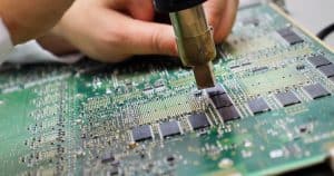
During fabrication, the board house plates nickel first, then gold.
The gold fingers remain unmasked during plating to achieve the correct finish.
After plating, the contacts undergo inspection for thickness, smoothness, and adhesion.
Following these steps yields durable, standards-compliant gold fingers.
It also minimizes production delays and rework.
Common Mistakes to Avoid
-
Insufficient Plating Thickness: Leads to rapid wear and connection issues.
-
Wrong Finger Spacing: Causes poor mating with connectors.
-
No Edge Bevel: Increases insertion force and risk of damage.
-
Mask Overlaps: Prevents proper plating and leaves bare copper exposed.
-
Missing Documentation: Confuses the manufacturer and delays production.
Avoiding these mistakes saves time and cost.
Clear communication with the PCB fabricator is essential.
Designers should review connector datasheets carefully before finalizing layouts.
Using checklists and design reviews can catch these errors early.
This is especially important for high-volume or safety-critical products.
Benefits of Gold Fingers in PCBs
Gold fingers offer multiple advantages:
-
Superior Conductivity: Ensures stable signal and power transfer.
-
Corrosion Resistance: Protects contacts in harsh environments.
-
Long Lifespan: Handles thousands of insertion cycles.
-
Standard Compatibility: Works with widely available edge connectors.
-
Improved Product Quality: Reduces returns and warranty claims.
These benefits justify the higher cost of gold plating.
When specified correctly, gold fingers reduce long-term maintenance costs.
They also improve customer satisfaction by ensuring reliable performance.
In short, gold fingers are a strategic design choice.
They protect your PCB investment and extend product longevity.
Final Thoughts
PCB gold fingers are small features with a large impact.
Designing them correctly ensures strong, reliable connections over time.
This requires understanding their function, following industry standards, and avoiding common mistakes.
By planning early, specifying proper materials, and testing thoroughly, designers achieve consistent results.
Gold fingers may increase upfront costs but provide superior performance and durability.
Readers who apply these guidelines can produce boards that meet demanding applications.
Whether for consumer electronics or mission-critical systems, gold fingers are key to quality.
FAQs
Q1: What is the typical thickness of gold plating on PCB gold fingers?
Usually between 30–50 microinches of hard gold over 100–150 microinches of nickel.
Q2: Why is the edge of a PCB beveled near gold fingers?
Beveling reduces insertion force and prevents connector damage.
Q3: Are there standards for PCB gold fingers?
Yes. IPC-A-600 and IPC-6012 outline quality and performance requirements.
Q4: Can ENIG (Electroless Nickel Immersion Gold) replace hard gold for gold fingers?
No. ENIG is softer and unsuitable for repeated insertions. Hard gold is required.
Q5: How many insertion cycles can PCB gold fingers handle?
Typically thousands of cycles, depending on plating thickness and usage conditions.

