


Electronic manufacturers prefer multilayer PCBs to single-layer PCBs as they provide more signal integrity. Based on the required complexity level, circuit boards vary from two to eight layers – each layer increase introduces two more layers. 2-layer PCBs are the most common multilayer circuit boards, and they contain interconnects on the upper and lower parts.
The difference in the number of layers among multilayer PCBs creates differences in their capacity and application. This article will dig deep into the differences between 2-layered and 4-layered PCBs and when to choose a 2-layer board over a 4-layer board.
Difference Between a 2-Layer PCB and a 4-Layer PCB
Comparing Stackups
The 2-layer circuit board stackup is clearly defined. The top layer is usually the signal layer, while the bottom layer is a thick layer containing copper material, which sums to approximately 1oZ. However, these specifications are applicable in a PCB with a final thickness of about 0.062 in and ±10%. These measurements vary according to the preferred parameters for custom boards.
Contrary to the 2-layer PCB, the 4-layer PCB is a bit complex. Two internal layers are placed between the top and bottom layers. The top signal layer is followed by a prepreg layer, which in turn is followed by the inner plane layer. The inner layer comprises a primary sublayer and inner layer 2. Lastly, we have the bottom layer, which also acts as a signal layer.
Comparing Designs
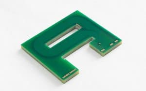
A 2-layer board design offers a more extensive surface area to accommodate a conductor pattern- it is almost twice as extensive as that of a 1-layer board. 2-layer PCBs also use vias to create electrical contacts. This facilitates the routing of traces to access the other PCB side.

An example of a 2-layer PCB design. Source
On the other hand, a 4-layer board design actually offers more surface area to create traces than 2-layer PCBs. A 4-layer PCB is created by applying heat and pressure to multiple double-sided boards, forming a prepreg layer in between. The prepreg acts as a dielectric between the board layers.

A 4-layer PCB design, source
Comparing Functionality
If you use microstrip traces with ground planes, a 2-layer board offers more functionality because it doesn’t experience transmission delays. However, a 4-layer board design with a ground plane, VCC plane, and two signal layers is more powerful despite facing impedance and transmission delays.
Comparing Cost
A 4-layer PCB is a bit expensive because of the design density and higher sensitivity levels. The high signal integrity obtained by minimizing alteration and transmission levels also contributes to the high cost of 4-layer PCBs.
Comparing the Creation of Prototypes
The need for creating a high-quality board can easily be achieved through prototyping. While a standard 4-layer board prototype is more complex than a 2-layer PCB prototype, automated software such as Gerber accelerates the creation of prototypes. The software has multiple preset parameters, like PCB thickness, aperture thickness, PCB finishing, etc. Furthermore, the use of Gerber software simplifies the manufacturing of custom boards.
Outsourcing to a PCB service provider that supports PCB prototyping is also an economical way of producing custom circuit board prototypes. For example, MKTPCB’s PCB prototyping service is supported by reliable manufacturing lines, offers prompt and free online quotes, and accepts Gerber files. We provide fast PCB prototyping services for customer designs while sticking to high-quality international manufacturing standards.
When to Choose a 2-Layer PCB Over a 4-Layer PCB
Picking a 2-layer PCB against a 4-layer PCB requires you to consider some important parameters. This section highlights the points you need to consider when choosing a 2-layer over a 4-layer board:
The optimum functionality constraint in inadequate space: Electronic design requires selecting the maximum size of internal parts. 4-layer PCBs are widely used in electronics because they are highly functional and compact. Generally, small and high-performing devices like smartphones work better with 4-layer boards.
More intricate functionality in electronics: 4-layer boards provide excellent support for electronics designed to provide complex and multiple functionalities. Hence, a 4-layer board is the better option when you want your electronics to be multi-functional.
Enhanced device durability: 4-layer boards offer enhanced device durability over 2-layer boards. Electronics fitted with 4-layer PCBs continue to function well throughout their lifespan due to the reliable performance of 4-layer designs.
Device affordability: Regarding device cost, 2-layer boards are cheaper than 4-layer PCBs. These PCBs involve low production costs and are ideal for low-budget electronics.
Quick product development: When designing electronics on short deadlines, you should choose 2-layer PCBs over 4-layer boards. The former is quick to produce because of a less complex design that guarantees easy rolling out of products.
Apart from the above factors, you should also consider the operating efficiency, signal transmission design, and density specifications.
Advantages of 2-Layer PCBs
2-layer circuit board sheets are commonly applied in consumer and computer electronics. They allow a higher thickness in segments and simplify the laying of tracks. Just like standard PCBs, 2-layer PCBs consist of the non-conductive substrate material. Two PCB layers allow a higher component thickness. This is because designers have a whole extra layer to add tracks to interface the segments, creating room on the other layer to mount components or introduce extra functionalities closely.
Another advantage of using 2-layer PCBs is the warmth distribution that the extra layer brings. This is achieved by boring through the copper to create tracks, sparing the extra layer instead of deleting it.
Typical Applications of 2-Layer PCBs
There are similar multiple use cases for old and new designs. Differences in SMT, ultra-high copper fabrication, extreme temperature differences, solder mask, and immersion techniques are a few cases of 2-layer PCB applications. 2-layer PCBs are widely used in the computer industry and consumer electronics, including radios, cameras, smartphones, wearables, and televisions. Beyond these applications, they are also utilized in many other fields, such as:
Medical equipment: 2-layer PCBs are complex and have high functionality, facilitating the performance of various medical research tests. Most medical testing equipment uses dense PCBs to perform even the most precise and complex tests. The thick component mounting allows designers to create smaller medical devices that can be inserted into the human body quickly and safely. 2-layer PCBs are widely used in various medical instruments, including pacemakers, CT scan machines, and X-ray equipment.
2-layer circuit boards are used in powerful industrial machines due to their high performance. The thick copper layers are ideal for engine regulators, high-current battery chargers, and load analyzers.
Telecommunications: Telecommunication equipment often uses 2-layer circuit boards in various applications, like signal broadcasting, GPS, and satellite functioning. This is because these boards have high performance and miniaturized sizes.
LED lighting designs are becoming less common due to their low power use and high energy output. As a result, aluminum PCBs are now less used in lighting. Instead, 2-layer PCBs with aluminum substrates are preferred for high-lumen LEDs and other lighting applications.
Automotive and aerospace industries: These two industries are making good use of multilayer PCBs because of their highly adaptive features. The features enable them to tolerate high vibrations and extreme temperatures that are common in these two industries. Depending on the requirements and plans, 2-layer boards are also lightweight, making them ideal for mobility applications.
2-Layer PCB Manufacturing and Assembly at Competitive Market Prices
With the current technological advancements and the demand for high-performing PCBs, you should exploit these trends and focus more on PCB functionality. Partnering with a reliable 2-layer PCB manufacturer and assembler should be part of your business development plans. With quality 2-layer PCBs, you will position yourself as a market leader in the production of high-performing electronics. MKTPCB can assist you in getting there.
MKTPCB is a leading PCB manufacturer and assembler based in Shenzhen, China. We also offer supportive PCB services such as component sourcing, quality testing, and shipping while adhering to the IPC, ISO, and RoHS standards. We will guide you throughout the PCB production process, offering expertise and clearing any doubt in our manufacturing capacities. In the last decade, we have manufactured thousands of 2-layer PCBs for various clients globally. MKTPCB engineers have a rich experience to actualize your dreams no matter the complexity of your design or application requirements.

