


In today’s fast-paced electronics industry, innovation is driven by miniaturization, speed, and reliability. Surface Mount Technology (SMT) has emerged as a cornerstone of modern PCB (Printed Circuit Board) manufacturing, playing a pivotal role in how electronic components are assembled. But what is SMT in PCB, and why does it matter so much?
Table of Contents
ToggleThis guide will give you a detailed understanding of SMT, how it compares to other mounting techniques, and why it’s the preferred choice in modern electronics.
What Is SMT in PCB?
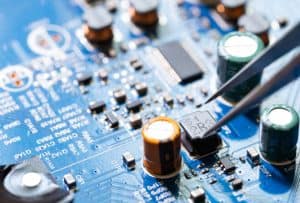
SMT (Surface Mount Technology) in PCB is a method of mounting electronic components directly onto the surface of printed circuit boards. Unlike traditional through-hole technology, where component leads are inserted into drilled holes, SMT places components—known as Surface Mount Devices (SMDs)—directly on the PCB surface.
This method enables higher component density, reduced size, faster production, and improved electrical performance.
The Importance of SMT in Modern Electronics
SMT is not just a manufacturing technique—it’s a revolution in electronic design. From smartphones and smartwatches to industrial control systems, SMT is at the heart of compact, high-performance electronics.
By eliminating the need for hole drilling and allowing for double-sided component mounting, SMT has drastically improved efficiency in PCB assembly processes.
SMT PCB vs Through-Hole: What’s the Difference?
| Feature | SMT PCB | Through-Hole PCB |
| Mounting Style | Surface mount | Pin-through-hole |
| Board Space | Saves space | Requires more space |
| Assembly Speed | Faster | Slower |
| Reliability in Vibration | Less reliable | More reliable |
| Cost | Lower for high-volume | Higher due to manual insertion |
| Use Case | Smartphones, laptops | Aerospace, military, power systems |
SMT PCB vs Through-Hole is a frequent comparison in PCB design. SMT is ideal for high-speed, high-volume manufacturing, while through-hole is preferred where mechanical strength is crucial.
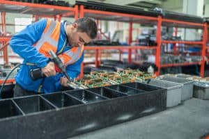
The SMT Assembly Process in PCB Manufacturing
The SMT assembly process PCB follows a series of well-defined steps to ensure precision and reliability. Here’s a breakdown:
1. Stencil Printing
A solder paste stencil is placed over the board, and solder paste is applied to the exposed pads. This step determines solder placement accuracy.
Learn more about stencils and how they help at MKTPCB SMT Stencil Process
2. Pick and Place
SMT machines place components accurately onto the solder-pasted pads using robotic arms guided by CAD data.
3. Reflow Soldering
The board passes through a reflow oven where solder paste melts, bonding components to the PCB.
4. Inspection
Techniques such as AOI (Automated Optical Inspection) and X-ray are used to check for misalignments, bridges, and cold solder joints.
5. Functional Testing
Final testing ensures the board works as intended before packaging and delivery.
SMT Reflow Soldering PCB: Why It’s Critical
SMT reflow soldering PCB is a thermal process where the board, after pick-and-place, is heated in a reflow oven. The solder paste melts and forms permanent electrical and mechanical connections.
There are typically four stages in a reflow oven:
- Preheat Zone
- Soak Zone
- Reflow Zone
- Cooling Zone
Proper profiling ensures components aren’t damaged, and solder joints are strong and defect-free.
SMT Components in PCB
SMT components PCB are specially designed to be soldered onto flat surfaces. Common types include:
- Resistors
- Capacitors
- ICs (Integrated Circuits)
- Transistors
- Diodes
These are available in standardized packages like 0603, 0805, QFP, BGA, and more—allowing dense placement and reduced footprint.
Surface Mount Device PCB Types
There are multiple surface mount device PCB types, typically classified by function and package:
- Passive Components: Capacitors, resistors
- Active Components: Diodes, transistors
- IC Packages: QFN, BGA, SOIC, LGA
Each type has specific reflow temperature profiles and assembly requirements, contributing to the complexity and adaptability of SMT assembly.
SMT PCB Advantages and Disadvantages
Advantages
- Compact size: Perfect for miniaturized electronics
- Higher circuit density: Enables complex designs
- Faster assembly: Ideal for mass production
- Lower manufacturing cost: Reduced material usage
Disadvantages
- Difficult rework: Components are tiny and closely packed
- Thermal stress: Improper soldering can damage parts
- Less mechanical strength: Compared to through-hole
Understanding SMT PCB advantages and disadvantages helps in making informed decisions during PCB design and prototyping.
SMT PCB Equipment List
For professional SMT assembly, specialized equipment is essential. Here’s a quick SMT PCB equipment list:
- Solder Paste Printer / Stencil Printer
- Pick and Place Machine
- Reflow Oven
- AOI (Automated Optical Inspection) System
- X-Ray Inspection Machine
- Solder Paste Inspection (SPI) System
- ESD-safe Workstations
- Conveyor Belts and PCB Handling Tools
These tools ensure high accuracy, consistency, and quality in the SMT PCB assembly process.
SMT PCB Miniaturization Benefits
One of the biggest appeals of SMT is miniaturization. As electronic devices become smaller and more powerful, SMT enables:
- Compact circuit designs
- Lighter weight
- Higher speed due to shorter signal paths
- Lower parasitic inductance and capacitance
These SMT PCB miniaturization benefits are why you’ll find SMT used in wearables, medical implants, IoT devices, and more.
SMT vs THT PCB: Final Thoughts
Still comparing SMT vs THT PCB? Here’s a quick summary:
- Use SMT when miniaturization, cost, and speed matter.
- Use THT when durability, ruggedness, and stress resistance are key.
In practice, hybrid designs are common—critical components use through-hole, while the rest use SMT for space and efficiency.
PCB = SMT Process Overview
When we talk about PCB = SMT process overview, we mean a fully integrated system where the PCB is designed, manufactured, and assembled using SMT techniques. This process includes:
- PCB design for SMT
- Panelization and stencil design
- Component selection
- PCB fabrication
- Solder paste printing
- Pick and place
- Reflow soldering
- Inspection and testing
This end-to-end approach ensures quality and reduces turnaround time in high-volume manufacturing.
FAQs – Surface Mount Technology PCB
What is the difference between SMT and SMD in PCB?
SMT (Surface Mount Technology) is the process used to mount components, while SMD (Surface Mount Device) refers to the actual components mounted via SMT. Think of SMT as the technique and SMDs as the components.
Why is SMT better than through‑hole technology?
SMT offers faster assembly, compact size, cost savings, and high-speed automation—ideal for modern electronics. Through-hole is better for high-stress or high-power applications but lacks scalability.
How does the SMT soldering process work on a PCB?
The SMT soldering process involves applying solder paste using a stencil, placing SMDs on the board, then heating it in a reflow oven to melt the paste and secure the components.
What are the main disadvantages of SMT assembly on PCB?
The main disadvantages include:
- Difficult manual repairs
- Limited mechanical strength
- Sensitivity to heat during reflow
However, these are manageable with proper design and tools.
What equipment is needed for SMT PCB assembly?
You’ll need:
- Stencil printer
- Pick and place machine
- Reflow oven
- AOI system
- X-ray inspection (optional)
- Solder paste inspection
These ensure high-precision assembly.
Final Thoughts
So, what is SMT in PCB—and why does it matter? It matters because it has transformed electronics manufacturing by enabling miniaturization, automation, and reliability. Understanding the nuances of SMT vs through-hole, the SMT assembly process, and the associated equipment and component types empowers designers and manufacturers to create advanced, compact, and efficient PCBs.
If you’re exploring high-quality SMT PCB manufacturing or stencil solutions, visit MKTPCB’s SMT Stencil Services and take your electronics project to the next level.

