


Printed circuit boards (PCBs) are the heart of modern electronics, powering everything from smartphones to medical devices. But have you ever wondered what goes into the PCB manufacturing process?
Table of Contents
ToggleIn this comprehensive guide, we’ll explore the key steps involved in PCB board manufacturing, the materials used, testing methods, quality control standards, and the cost factors that influence production. Whether you’re a design engineer, a buyer, or simply curious, this article will walk you through the entire PCB fabrication process—from PCB design to manufacturing.
1. Introduction to PCB Manufacturing
The PCB manufacturing process is a complex, multi-step journey that transforms a design file into a fully functioning printed circuit board. It requires advanced machinery, high-quality materials, strict adherence to PCB manufacturing standards, and a robust quality control framework.
Why is it Important?
The reliability and performance of electronic devices heavily depend on how well the PCB is manufactured. Poor-quality PCBs can result in device failures, higher costs, and longer time-to-market.
2. Step-by-Step PCB Fabrication Process
The PCB fabrication steps involve converting a circuit design into a physical board. Below is a breakdown of the key stages:
1. Design and Output File Preparation
Everything starts with the PCB design. Designers use CAD software to create layout files, which are then converted into Gerber files—the industry standard format for PCB manufacturing.
2. Printing the PCB Design
Using a photoplotter, the PCB layout is printed onto a film. This film serves as a blueprint for each layer of the board.
3. Creating the Substrate
The core base of the PCB is made from fiberglass (FR4), which is coated with copper on both sides. This becomes the foundation upon which all components are added.
4. Laminating and Imaging
The copper-clad laminate is covered with a photoresist layer, then exposed to UV light through the film. This step etches the design onto the copper.
5. Etching the Inner Layers
Using chemicals like ferric chloride, the unwanted copper is removed, leaving only the desired circuit paths.
6. Layer Alignment and Lamination
For multi-layer PCBs, the inner layers are stacked and laminated under heat and pressure to form a unified board.
7. Drilling
Precision drilling creates holes for vias and component leads. CNC machines ensure extreme accuracy.
8. Plating
The drilled holes are plated with copper to establish electrical connectivity between layers.
9. Solder Mask Application
A protective solder mask is applied to prevent short circuits and to insulate the board, leaving only the component pads exposed.
10. Silkscreen Printing
Component labels, logos, and markings are added using a silkscreen process.
11. Surface Finish
To prevent oxidation and ensure solderability, a surface finish such as HASL, ENIG, or OSP is applied.
12. Final Cutting and Profiling
The PCB is cut into its final shape using a router or V-cut machine.
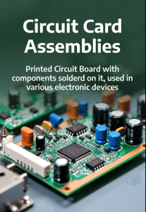
3. PCB Assembly Process Explained
Once the PCB is fabricated, the PCB assembly process begins. It involves placing and soldering electronic components onto the board.
Key Steps:
- Solder Paste Application
- Pick and Place of Components
- Reflow Soldering
- Manual or Wave Soldering (for through-hole components)
- Inspection and Quality Testing
The choice of assembly method (SMT, THT, or mixed) depends on the design complexity and intended application.
4. PCB Prototyping Process
Before mass production, a PCB prototyping process is used to validate design functionality and manufacturability.
Why Prototype?
- Reduce design errors
- Improve performance
- Accelerate time to market
Prototyping typically uses faster turnaround times, small batch sizes, and simplified testing. It’s a crucial step to catch issues early in the development cycle.
5. PCB Testing Methods
High-reliability electronics require robust PCB testing methods. Here’s an overview:
1. Automated Optical Inspection (AOI)
AOI uses high-resolution cameras to detect defects such as missing components, solder bridges, or misalignments. It’s essential for high-volume SMT production.
2. In-Circuit Testing (ICT)
ICT uses probes to test electrical characteristics such as resistance, capacitance, and current flow. It helps verify the functionality of individual components.
3. Flying Probe Testing
Ideal for prototypes or low-volume runs, this test method uses movable probes to access test points without needing a custom fixture.
4. Functional Testing
The final test simulates real-world operating conditions to verify that the PCB performs as expected.
6. PCB Manufacturing Materials
Understanding PCB manufacturing materials is key to building reliable electronics. Common materials include:
| Material | Purpose |
| FR4 (Fiberglass) | Insulating substrate |
| Copper | Conductive pathways |
| Solder Mask | Protection and insulation |
| Silkscreen Ink | Marking components |
| Surface Finish | Prevent oxidation (ENIG, HASL, OSP) |
Special materials like polyimide or metal-core substrates are used in high-temperature or high-power applications.
7. PCB Manufacturing Cost Factors
Several PCB manufacturing cost factors affect the final price:
1. Board Size and Layer Count
More layers and larger boards require more materials and labor.
2. Complexity of Design
Dense layouts or fine-pitch components increase difficulty and cost.
3. Surface Finish and Materials
Advanced finishes like ENIG are more expensive than HASL.
4. Volume and Lead Time
High-volume and flexible timelines reduce per-unit costs.
5. Testing and Certification
Extra quality checks and compliance with specific PCB manufacturing standards (e.g., IPC Class 3) increase production costs.
8. PCB Manufacturing Standards and Quality Control
To ensure reliability and consistency, manufacturers follow global PCB manufacturing standards, including:
- IPC-A-600: Acceptability of printed boards
- IPC-6012: Qualification and performance of rigid boards
- ISO 9001: General quality management
- RoHS/REACH: Environmental compliance
Quality Control Practices:
- Incoming material inspection
- In-process AOI and ICT testing
- Final inspection and packaging
A strict PCB manufacturing quality control process helps reduce returns and field failures, especially for mission-critical applications like aerospace or medical devices.
9. Frequently Asked Questions (FAQs)
What are the main steps involved in the PCB manufacturing process?
The key steps include design file preparation, copper etching, layer lamination, drilling, plating, solder masking, silkscreen printing, and surface finishing. After fabrication, the board is assembled and tested.
How long does it typically take to manufacture a PCB?
For prototypes, the process can take 2–5 business days, while high-volume production may require 1–3 weeks, depending on complexity and lead times.
What materials are commonly used in PCB manufacturing?
Common materials include FR4 fiberglass, copper, solder mask, and various surface finishes like ENIG and HASL. Specialized applications may use ceramic or metal-core substrates.
What are the common testing methods for PCBs?
Standard tests include AOI, in-circuit testing (ICT), flying probe testing, and functional testing to ensure quality and performance.
What factors influence the cost of PCB manufacturing?
Cost factors include layer count, board size, design complexity, material choice, volume, turnaround time, and testing requirements.
- Final Thoughts
Understanding the PCB manufacturing process is essential for engineers, product designers, and procurement teams. From design to assembly and final inspection, each step must be meticulously executed to produce high-quality boards that meet performance standards and customer expectations.
At MKTPCB, we provide full-service PCB manufacturing, including prototyping, assembly, and testing—all under one roof. With a commitment to quality, innovation, and timely delivery, we’re here to bring your designs to life.

