In today’s digitally driven world, electronics are the foundation of everything from smartphones and medical devices to industrial machinery and automotive systems. At the core of these devices lies a critical process known as Printed Circuit Board Assembly (PCBA). This process transforms a bare PCB into a functional electronic board—complete with all necessary components—capable of powering the most advanced technologies.
Table of Contents
ToggleUnderstanding the PCB assembly process is vital for engineers, product developers, and businesses seeking reliable electronic solutions. In this article, we’ll explore what PCBA entails, why it’s essential in modern electronics, and how different technologies like surface mount technology (SMT), through-hole assembly, and automated optical inspection (AOI) shape the future of manufacturing.
What Is the PCB Assembly Process?
The PCB assembly process refers to the method of soldering and assembling electronic components onto a bare printed circuit board (PCB) to create a working electronic device. It includes both manual and automated steps, depending on the complexity and volume of the boards.
There are three primary stages in the PCBA process:
- Solder Paste Application – Solder paste is applied to the areas where components will be mounted.
- Component Placement – Using a pick and place machine, components are placed accurately on the board.
- Soldering – The board is passed through a reflow soldering oven or wave soldering system to secure components in place.
Once soldering is completed, PCB assembly inspection and PCB assembly testing methods are employed to ensure quality and functionality.
Surface Mount Technology (SMT)
Surface mount technology (SMT) is the dominant technique used in modern PCB assembly. SMT involves placing components directly onto the surface of the board, eliminating the need for drilled holes.
Benefits of SMT in PCB Assembly:
- Higher component density
- Reduced manufacturing costs
- Faster production speeds
- Enhanced performance in compact devices
SMT is ideal for high-volume production and is often paired with automated optical inspection tools for better quality control.
Through-Hole Assembly
Despite the popularity of SMT, through-hole assembly remains relevant for applications requiring robust mechanical bonds or high-power components.
In this method, leads of components are inserted into drilled holes and soldered from the opposite side of the PCB. Through-hole assembly is often used in:
- Aerospace and defense applications
- High-stress environments
- Prototyping and testing
Combining SMT and through-hole techniques often results in a hybrid PCB assembly process to leverage the advantages of both.
Pick and Place Machine: Precision and Speed
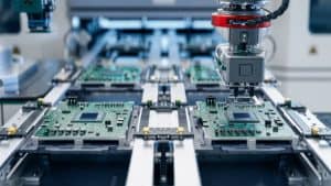
A pick and place machine is an automated system that selects components from reels or trays and accurately places them on the PCB.
Key Features:
- High-speed placement (thousands of components per hour)
- Accurate positioning
- Versatile component handling (from tiny resistors to large ICs)
The use of pick and place machines minimizes human error and enhances the consistency of PCB assemblies.
Reflow Soldering: Securing Surface-Mounted Components
Reflow soldering is a key process in SMT-based assembly. Once the components are placed, the board is passed through a reflow oven where the solder paste melts and forms strong electrical and mechanical joints.
Steps in Reflow Soldering:
- Preheat Zone – Gradually raises the temperature.
- Soak Zone – Ensures thermal equilibrium.
- Reflow Zone – Melts the solder paste.
- Cooling Zone – Solidifies the solder joints.
Proper thermal profiling during reflow soldering is essential to prevent PCB assembly defects such as cold solder joints or tombstoning.
PCB Assembly Testing: Ensuring Functionality and Reliability
PCB assembly testing is critical for identifying defects, ensuring performance, and meeting regulatory standards. Skipping this step can lead to costly field failures.
Common PCB Assembly Testing Methods:
- In-Circuit Testing (ICT) – Tests individual components.
- Functional Testing – Verifies the final product behavior.
- Flying Probe Testing – Ideal for low-volume production.
- Boundary Scan Testing – Suitable for complex BGA packages.
All these PCB assembly testing methods help in detecting faults like short circuits, open circuits, and misaligned components.
Automated Optical Inspection (AOI)
Automated optical inspection (AOI) is a non-contact method used to visually inspect PCBs after soldering. AOI systems use high-resolution cameras to scan boards for anomalies.
What Does AOI Detect?
- Missing components
- Misaligned components
- Soldering defects
- Polarity errors
AOI is crucial for maintaining product quality, especially in high-volume PCB assembly services.
Common PCB Assembly Defects and Their Prevention
Even with advanced technologies, PCB assembly defects can still occur. Some of the most common include:
1. Solder Bridges
Caused by excess solder connecting adjacent pads. Prevented by accurate solder paste application.
2. Tombstoning
Occurs when a component lifts from one pad during reflow. Controlled by adjusting thermal profiles.
3. Cold Solder Joints
Weak connections due to insufficient heat. Resolved by optimizing reflow soldering settings.
4. Misaligned Components
Often due to poor handling or pick and place errors. Can be corrected using AOI and machine calibration.
By implementing stringent quality control and testing procedures, these defects can be minimized effectively.
PCB Assembly Cost: Factors to Consider
Several factors influence PCB assembly cost, including:
- Component complexity – Fine-pitch or high-pin-count components increase cost.
- Board layers and size – Multilayer or large boards are more expensive.
- Assembly volume – Higher quantities reduce per-unit cost.
- Testing requirements – More rigorous testing adds to the cost.
- Turnaround time – Faster delivery usually incurs a premium.
Understanding these variables helps in budgeting and choosing the right PCB assembly services for your project.
Why PCB Assembly Matters in Modern Electronics
The PCB assembly process is the backbone of modern electronic manufacturing. It ensures that devices are:
- Compact and reliable
- Cost-effective to produce
- Scalable in volume
- Compliant with international standards
Without high-quality PCBA, critical industries like medical, automotive, and aerospace would not function efficiently.
- Companies like MKTPCB specialize in delivering comprehensive PCB assembly services, ensuring each board meets precise quality and performance criteria.
FAQs
What is the difference between SMT and through-hole assembly?
Surface mount technology (SMT) mounts components directly onto the surface of the PCB, ideal for compact, high-speed applications. Through-hole assembly involves inserting leads through holes and soldering them on the opposite side, providing stronger mechanical bonds, especially in high-stress environments.
How does automated optical inspection (AOI) work in PCB assembly?
AOI uses high-definition cameras and image processing algorithms to scan PCBs for defects such as missing components, solder bridges, and misalignments. It is a fast, accurate, and essential step in automated PCB quality control.
What are common defects in PCB assembly and how can they be prevented?
Common PCB assembly defects include solder bridges, cold solder joints, tombstoning, and misaligned components. Prevention involves accurate solder paste application, proper reflow soldering profiles, and inspection using AOI and functional testing.
What factors influence the cost of PCB assembly?
PCB assembly cost is influenced by component types, board complexity, production volume, turnaround time, and testing requirements. Custom or low-volume runs typically have higher costs due to setup and sourcing complexities.
Why is testing crucial in the PCB assembly process?
PCB assembly testing ensures that every board functions correctly before deployment. It helps detect faults early, reduces product recalls, and increases overall reliability and customer satisfaction.
Conclusion
The PCB assembly process is a complex yet crucial part of electronic manufacturing. By combining technologies like surface mount technology (SMT), through-hole assembly, pick and place machines, reflow soldering, and automated optical inspection (AOI), manufacturers can create highly reliable and functional electronic products.
Quality PCB assembly services, like those offered by MKTPCB, are essential for industries seeking dependable electronic solutions. By understanding the key aspects of PCBA—from design and placement to testing and cost factors—you can ensure your next project meets the highest standards of performance and reliability.
Ready to start your next PCB assembly project?
Contact MKTPCB today for expert guidance, top-tier services, and reliable solutions tailored to your application.


