


Common PCB Defects and Fixes
Printed Circuit Boards (PCBs) are the backbone of electronic devices.
However, even small errors in design or manufacturing can cause major failures.
Understanding common PCB defects and knowing how to fix them can save time, cost, and product reliability.
Introduction to PCB Defects
PCB defects occur due to various factors, including poor soldering, incorrect design parameters, or manufacturing inconsistencies.
These issues affect electrical performance and reliability, leading to device malfunction or complete failure.

During production, the smallest deviation in trace width, hole alignment, or solder application can result in open or short circuits.
Environmental conditions such as humidity and temperature can also contribute to defects.
Identifying defects early using inspection tools like Automated Optical Inspection (AOI) or X-ray testing helps reduce scrap and rework.
The goal isn’t only to fix defects but to understand their root cause to prevent recurrence.
Manufacturers and engineers can improve PCB quality by combining thorough design checks, advanced fabrication processes, and strong quality assurance methods.
Let’s explore the most common defects in PCB manufacturing and design—and how to fix them effectively.
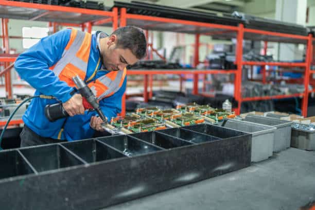
Common PCB Manufacturing Defects
Manufacturing defects often arise during soldering, component placement, or etching.
These errors may not be visible at first glance, but can impact performance.
Solder Bridges
Solder bridges occur when excess solder connects two adjacent pads or leads, creating a short circuit.
They are often caused by too much solder paste or misaligned stencils.
To fix this, use solder wick or a solder sucker to remove the bridge and clean the board with isopropyl alcohol.
Prevent recurrence by using precise solder paste application and proper reflow temperature profiles.
Cold Solder Joints
A cold solder joint forms when solder fails to melt completely, resulting in weak connections.
They appear dull or cracked and can lead to intermittent signal loss.
Fix the issue by reheating the joint with the correct temperature and adding a small amount of fresh solder.
Ensure soldering irons are well-calibrated and components are properly seated before soldering.
Open Circuit
An open circuit happens when a connection is broken, stopping current flow.
This may result from poor solder joints or damaged traces.
You can repair it using a conductive pen or wire to bridge the gap.
To prevent this, maintain proper solder coverage and avoid mechanical stress during assembly.
Short Circuits
Short circuits occur when two unintended connections touch each other, causing excess current flow.
Common causes include solder splashes, debris, or incorrect component orientation.
Fix by identifying the bridge using a multimeter and carefully removing the excess solder.
Maintaining a clean workspace is the best prevention method.
Component Misalignment
Misaligned components affect both aesthetics and performance.
This defect usually happens due to incorrect pick-and-place machine calibration.
Realign or re-solder the affected parts.
Verify machine settings and ensure correct pad designs to minimize such issues.
Common PCB Design Defects
Design-level defects occur before manufacturing even begins.
They are often the result of poor layout planning or ignoring manufacturing tolerances.
Trace Width Issues
Traces that are too thin cannot handle current, leading to overheating or breaks.
Follow IPC-2221 standards to determine the minimum trace width for your design.
Adjust the width in the PCB layout software and verify during prototype testing.
Inadequate Copper Thickness
Insufficient copper affects current capacity and heat dissipation.
Use thicker copper layers for high-power applications.
Work closely with your PCB manufacturer to select suitable copper weights.
Poor Thermal Management
Without proper heat dissipation, components may overheat and fail.
Add thermal vias, heat sinks, and ground planes to distribute heat evenly.
Thermal analysis during design helps identify hotspots early.
Effective Fixes for PCB Defects
Fixing PCB defects starts with accurate detection.
Use visual inspection, AOI, and electrical testing to locate issues precisely.
Rework stations can address soldering defects, while conductive repair kits handle damaged traces.
Replace faulty components carefully to prevent heat damage.
For recurring defects, analyze production data to trace the root cause.
Document all issues and corrective actions for continuous improvement.
Establishing a feedback loop between the design and manufacturing teams ensures long-term quality.
This collaboration reduces production downtime and prevents costly recalls.
How to Prevent PCB Defects in Future Designs
Prevention is the most efficient approach to PCB defect management.
Use design-for-manufacturing (DFM) principles to reduce risks.
Follow IPC standards for layout, spacing, and soldering.
Collaborate with your PCB supplier to verify design compatibility before production.
Perform electrical tests and thermal analysis during the prototype phase.
Regularly calibrate equipment and ensure proper operator training.
A well-documented quality control checklist helps maintain consistency across all production stages.
Regular audits and process reviews further strengthen reliability and customer satisfaction.
Conclusion
Understanding and fixing PCB defects is crucial for reliable electronics.
From soldering mistakes to poor design choices, every issue can be traced, corrected, and prevented.
By maintaining strong quality control and design practices, manufacturers can minimize failures and ensure long-term performance.
For reliable PCB manufacturing and assembly solutions, visit MKTPCB’s About Page to learn how quality and precision shape every project.

