


Introduction
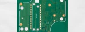
Heavy copper PCB manufacturing produces printed circuit boards with copper thicknesses far greater than standard PCBs — typically 3 oz/ft² (≈105 µm) and above, often 6 oz (≈210 µm), 10 oz (≈350 µm), or even thicker. These boards are essential for high-current, high-heat, and rugged applications such as power supplies, battery management systems, automotive electronics, industrial drives, and military equipment. This post outlines the manufacturing processes, material choices, design considerations, testing procedures, and advantages of heavy copper PCBs, enabling designers and engineers to make informed decisions.
What makes a PCB “heavy copper”?
A heavy copper PCB utilizes copper weight (measured in ounces per square foot or µm thickness) that is significantly greater than the typical 1 oz (≈35 µm) boards. Heavy copper is achieved by:

-
Using thicker copper foils or laminates
-
Electro-deposition (plating) to add copper to traces, planes, and through-holes
-
Selective copper plating to reinforce critical current paths and thermal paths
Why choose heavy copper PCBs?
Key reasons include:
-
High current capacity: Thick traces reduce trace resistance and voltage drop, handling high amperage without overheating.
-
Improved thermal performance: More copper increases heat spreading and lowers hotspot risk.
-
Mechanical durability: Thicker copper increases mechanical strength and resistance to wear in connectors and heavy pads.
-
Lower impedance and improved reliability: For power distribution networks, thicker copper provides stable, predictable behavior under load.
Typical applications
-
Power electronics (inverters, converters, UPS)
-
Automotive traction systems and EV power modules
-
Aerospace and defense equipment
-
Industrial motor controllers and welding machines
-
Battery management systems and power distribution assemblies
Manufacturing processes — step by step
1. Material selection
Start with suitable substrates and copper: FR-4, high-Tg laminates, metal-core (MCPCB) where required, and heavy copper clads (thick copper foil) or standard clads with planned plating.
2. Pattern imaging and etch (when using thick foils)
For very thick foils, you may use direct imaging. Etching thick copper is possible, but slower and less precise than plating — for many heavy copper boards, plating is preferred.
3. Build-up by electroplating (preferred)
Electroplating adds copper where needed:
-
Seed layer: A thin conductive layer (often by sputtering or chemical deposition) forms the base.
-
Photoresist & imaging: Apply photoresist and image the circuit pattern.
-
Electroplating: Copper is plated to the required thickness. Designers can selectively plate power traces, planes, and through-holes.
-
Strip resist and finish: Remove resist, clean, and apply surface finishes like HASL, ENIG, or OSP, depending on solderability/assembly needs.
Electroplating is more controllable and cost-effective for achieving very high copper weights.
4. Thru-hole plating and via creation
Through-holes and vias must be plated to carry currents between layers. Heavy copper boards often require multiple plating steps to ensure via reliability and low resistance.
5. Multilayer lamination under pressure
When building multilayers, thicker copper may affect the lamination profile — shop-floor attention to pressure, temperature, and prepreg thickness is critical to avoid voids or delamination.
6. Drilling and routing
Drills must be robust (often carbide) and process parameters adjusted to handle thick copper and tougher substrates. Tool wear and burr control are important.
7. Surface finish and protection
Choose finishes to match operational and assembly needs. For heavy copper subject to high current and mechanical stress, ENIG, immersion silver, or selective thicker finishes may be used. Conformal coating is common for environmental protection.
8. Testing and QA
-
Continuity & isolation testing
-
Thermal cycling & shock (for critical applications)
-
Current-stress tests (run high current to verify heating and voltage drop)
-
X-ray or cross-sectioning to check plating quality and via fill
-
IPC class inspections, depending on the quality level required (Class 2/3)
Design considerations & best practices
-
Specify copper weight clearly: Use oz/ft² and µm in the fabrication notes. Example: 6 oz (≈210 µm) on external layers.
-
Use wider traces: Calculate trace widths for desired current using IPC-2152 rather than older IPC-2221 tables for accurate results.
-
Plan copper pours & planes: Large copper areas help distribute heat but require careful thermal relief and balance to avoid warpage.
-
Avoid very narrow neck-downs in heavy copper areas: Sudden trace width reductions create hotspots.
-
Consider thermal vias / multiple vias: For heat transfer to internal planes or metal cores, add arrays of thermal vias with adequate annular rings and plating.
-
Adjust drill and annular ring specs: Thicker copper requires larger annular ring allowances and careful drill-to-pad clearances.
-
Account for plating tolerance: Electroplating thickness has tolerance; specify minimum and target thicknesses.
-
Lamination stack-up planning: Heavy copper changes pressure distribution — work with your fabricator on prepreg choices and lamination profile.
-
Test points & assembly: Use reinforced pads for screw terminals, busbars, and heavy connectors.
Cost trade-offs
Heavy copper PCBs are more expensive due to material, plating time, drilling wear, and processing challenges. However, they can reduce system costs by eliminating the need for discrete busbars, large soldered bars, or multiple parallel traces. Always perform a cost-vs-performance analysis.
Common defects and how to avoid them
-
Voids in plating: Use controlled plating chemistry and adequate agitation.
-
Delamination: Control lamination process and prepreg selection; avoid trapped stresses.
-
Burrs during drilling: Use proper drill speeds and replace worn tooling frequently.
-
Uneven plating: Maintain consistent current density and masking practices.
FAQs
Q1: What copper thickness qualifies as “heavy”?
A: While definitions vary, copper heavier than 3 oz/ft² (≈105 µm) is commonly called heavy copper. Many suppliers start marketing boards at 6 oz or above as heavy copper solutions.
Q2: Can heavy copper PCBs be multilayer?
A: Yes. Multilayer heavy copper PCBs are common but require careful lamination, prepreg selection, and process controls to prevent warpage and ensure reliable interlayer connections.
Q3: How do I calculate the trace width for high current?
A: Use IPC-2152 current carrying capacity charts or calculators that account for internal vs. external layers, temperature rise, and copper thickness. Many PCB CAD tools include calculators.
Q4: Are metal-core PCBs (MCPCBs) the same as heavy copper?
A: No. MCPCBs use a metal base (aluminum or copper) for thermal management; heavy copper PCBs simply use thicker copper. They solve related but different thermal/mechanical needs.
Q5: What surface finish is best for heavy copper?
A: Choice depends on assembly and environment. ENIG offers flatness and reliability; immersion silver provides good solderability. For very high-current connections, selective thick finishes or solder preforms may be used.
Q6: Is heavy copper plating reliable for automotive use?
A: Yes — when manufactured to automotive quality standards (e.g., AEC-Q related processes) and properly tested for thermal cycling and vibration, heavy copper PCBs are widely used in automotive power electronics.
Conclusion
Heavy copper PCB manufacturing enables robust, high-current, thermally efficient circuit boards essential for modern power electronics, EV systems, industrial drives, and other demanding applications. Success requires clear specification, careful design choices (trace width, thermal vias, laminates), and collaboration with experienced fabricators. While costs are higher than standard PCBs, the system-level benefits — simplified assemblies, improved reliability, and superior thermal handling — often justify the investment. If you’re designing for high currents or harsh environments, heavy copper is a strong candidate — get your stack-up and fabrication notes right, and test early and thoroughly.

