


LED applications—from lighting to displays—depend on reliable, thermally efficient circuit boards.
The performance, longevity, and cost of LED products hinge directly on the quality of the LED PCB.
In this article, we describe the manufacturing of LED PCBs: how they are built, what to watch for, and how to pick a supplier.
Engineers will gain clarity on materials, process steps, thermal management, quality controls, and market trends.
What Is LED PCB Manufacturing?
LED PCB manufacturing is the process of creating a printed circuit board designed specifically to support LEDs.
These boards often incorporate substrates and layouts optimized for heat dissipation, current carrying, and optical requirements.

They differ from standard PCBs by focusing on thermal paths, metal core usage, and special plating.
Manufacturing encompasses design input, substrate preparation, etching, plating, solder mask, finishing, and assembly readiness.
The goal is a board that ensures long LED life, uniform brightness, safe electrical performance, and manageable cost.
Materials & Substrate Options
FR-4 & Conventional Boards
FR-4 (glass epoxy) is inexpensive and common in general electronics.
It is usable for low-power LED boards or decorative lighting where heat is minimal.
However, its thermal conductivity is low (< 0.3 W/m·K).
Thus, for moderate to high power LEDs, FR-4 often fails to remove heat adequately.
It may be used for control circuitry sections rather than the LED mounting zones.
Aluminum / Metal Core PCBs
Metal core PCBs (MCPCBs) use aluminum or copper as a base metal.
They allow higher thermal conductivity (typically 2–3 W/m·K or more).
The metal core lies beneath dielectric and copper layers, giving a direct thermal path.
These are the most used boards for mid-to-high power LED modules.
Thickness, dielectric thickness, and copper layer thickness all influence thermal resistance and cost.
Ceramic Substrates
Ceramic substrates (alumina, aluminum nitride, SiC) offer high thermal conductivity (20–170 W/m·K).
They do not include a metal core but rely on the ceramic’s intrinsic conductance.
Ceramics resist warping, provide excellent insulation, and operate at high temperatures.
But they are more expensive and harder to process (brittle, requiring special handling).
Ceramics are preferred in high-reliability LED devices, automotive, and aerospace lighting.
Key Process Steps
Design & Layout
LED footprints, thermal vias, copper pours, and traces must be placed to minimize resistance.
Use thermal simulation tools to predict hot spots.
Define via size, spacing, number of layers, and thickness of copper.
Define the dielectric thickness above the metal core or between copper layers.
Include assembly tolerances, hole clearances, silkscreen, and solder mask constraints.
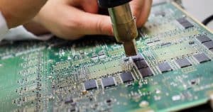
Drilling, Plating, Etching
Drilling creates holes for vias and through-holes (if any).
Plating adds a copper layer inside via barrels and onto surfaces.
Etching removes unwanted copper to define traces, pads, and planes.
Control of line width, spacing, and edge quality is critical to prevent defects.
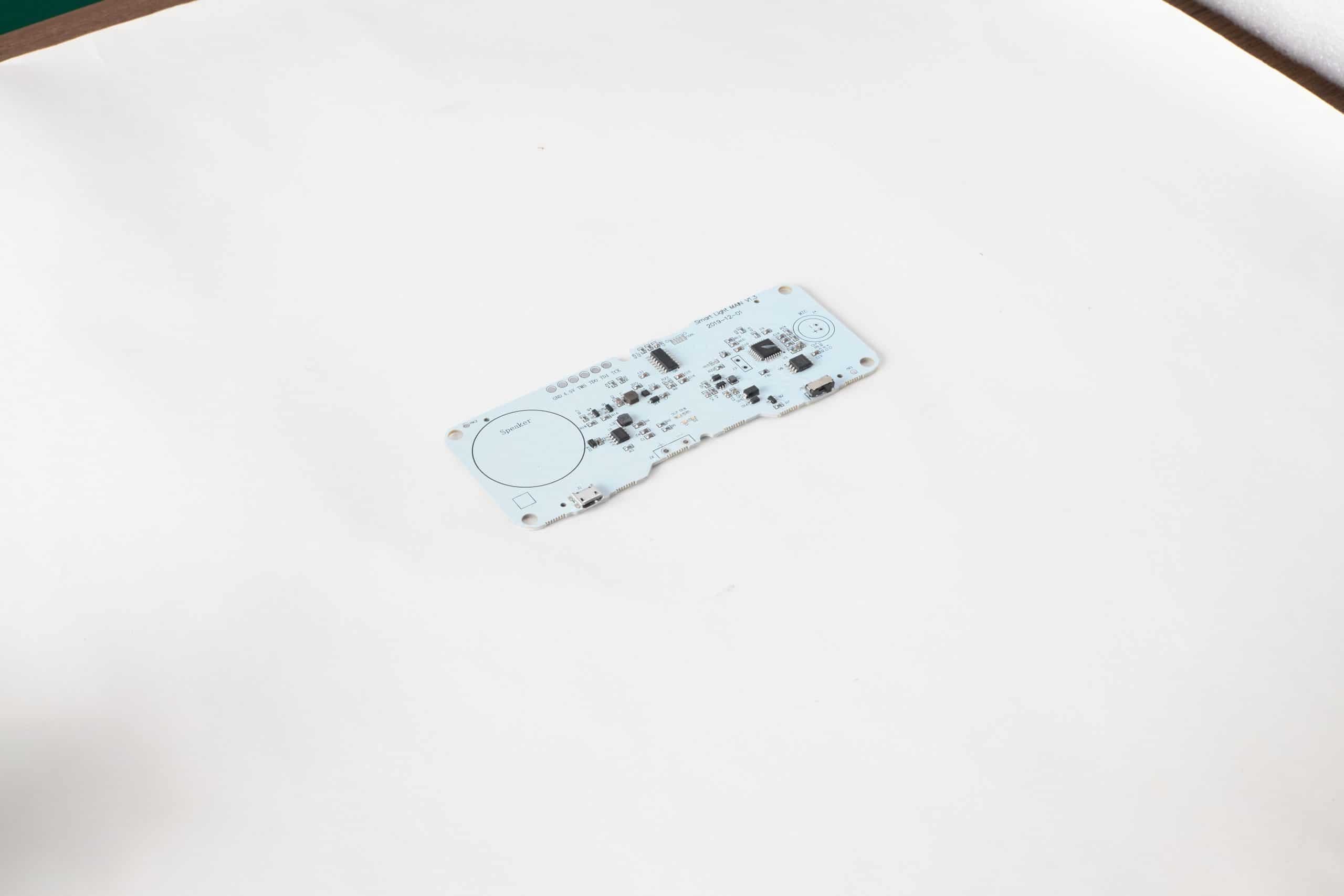
Solder Mask, Silkscreen
Apply solder mask to protect traces and prevent solder bridging.
Ensure mask alignment is precise, particularly around LEDs and pads.
Silkscreen adds text or markers (polarity, reference designators).
Select mask materials resistant to high reflow temperatures typical for LEDs.
Surface Finish & Testing
Finish options: HASL, ENIG, immersion silver, or OSP, depending on soldering needs.
Finish must be compatible with LED assembly methods (reflow, wave, etc.).
Electrical tests (continuity, isolation) verify correct connectivity.
Preliminary inspection includes measuring copper thickness, solder mask coverage.
Thermal Management in LED PCBs
Efficient heat removal is essential to prevent LED degradation.
Use thermal vias under LED pads to channel heat into the metal core or internal planes.
The dielectric layer thickness and its thermal conductivity control thermal resistance.
Optimize copper plane size; a larger area spreads heat more evenly.
Minimize hotspots by balancing current density and trace width.
Use thermal simulation software to validate the design before fabrication.
Ensure good interface between PCB and heat sinks or housings (e.g., TIM, adhesives).
Even small errors in thermal path design can shorten LED life dramatically.
Quality Control & Reliability
Thermal Cycling Tests
Expose boards to repeated temperature swings (e.g., –40 °C to 125 °C) to test fatigue.
Check for cracks, delamination, and changes in resistance.
Visual Inspection & X Ray
Inspect for delamination, voids, solder defects, and misalignment.
Use X-ray to evaluate buried vias, internal cracks, and hidden defects.
Life Testing
Operate LED assemblies under defined current and temperature to project lifespan.
Monitor lumen decay, failures over extended time.
Choosing a Supplier: Checklist
-
Experience with LED PCB types (metal core, ceramics)
-
Thermal simulation and design support
-
Capability: layer count, board thickness, via density
-
Quality certifications (ISO 9001, IPC compliance)
-
Testing capacities: thermal cycling, X-ray, life testing
-
Turnkey assembly options, logistics, and communication
-
Sample and prototyping support
-
Warranty, failure analysis practices
Cost Factors & Lead Time
Key cost drivers: substrate type (ceramic is expensive), copper thickness, via count, board size, and finishing method.
Complexity (fine traces, tight tolerances) raises cost.
Quantity: Prototyping is more expensive per unit than mass runs.
Lead times vary: basic metal core boards may take 5–10 days; ceramics take longer.
Testing, rework, and iteration add time.
Custom finishes or stringent QA increase both cost and delay.
Trends & Innovations in LED PCB Manufacturing
-
Embedded thermal materials (phase-change layers) for enhanced heat spreading
-
Additive manufacturing of metal layers (thicker copper, 3D structures)
-
Flexible LED PCBs (hybrid metal-flex) for curved lighting
-
Improved ceramic processes for lower-cost high-conductivity substrates
-
IoT-enabled monitoring of LED modules (sensors on PCB)
Conclusion
LED PCB manufacturing requires thoughtful material choice, precise process control, and rigorous testing.
Thermal design is the central challenge.
By choosing experienced suppliers, verifying capabilities, and aligning design with manufacturing realities, you can minimize risk.
Well-manufactured LED PCBs translate directly into higher reliability, performance, and customer satisfaction.

