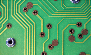
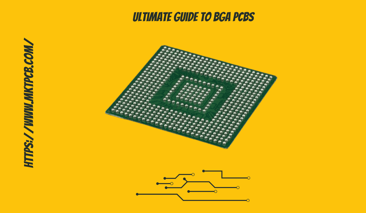
A BGA PCB refers to “a printed circuit board that incorporates Ball Grid Array packaging for its integrated circuits to ensure space efficiency and high connection density”. BGA technology is widely used in applications like microprocessors and memory chips. It is also leveraged to design integrated circuits found in modern electronic devices, including computers, smartphones, and various consumer electronics.
Table of Contents
ToggleIn this article, we’ll discuss everything, from BGA PCB types to design, layout, and overall benefits.
BGA PCB Types
There are different types of Ball Grid Array PCBs, each having its own set of benefits and challenges. Their choice often depends on the specific requirements of the application, including thermal management, space constraints, cost, and the need for high-density interconnections.
Let’s have a look at all major types of BGA PCBs for further elaborated details-
Plastic Ball Grid Array (PBGA)
Plastic Ball Grid Array (PBGA) emerges as a highly favored choice among BGA PCBs, primarily attributing its popularity to cost-effectiveness. It offers optimal thermal management, adeptly channeling heat away from the silicon die. All while ensuring enhanced performance reliability. Its architecture is innovative, allowing for a high density of interconnections. This remarkable feature makes PBGA it useful for devices like smartphones, gaming consoles, and PCs.

Ceramic Ball Grid Array (CBGA)
Ceramic Ball Grid Array (CBGA) is a high-performing BGA PCB that stands out for its unparalleled thermal stability and electrical prowess. Crafted from robust ceramic materials, CBGA guarantees an exceptional performance, especially in devices demanding high-temperature resilience. The low thermal resistance of CBGA translates into superior heat dissipation, a critical factor in maintaining system stability. Its reliability is unmatched, making it highly useful in industries like aerospace, military, and advanced telecommunications.

Tape Ball Grid Array (TBGA)
Tape Ball Grid Array (TBGA) presents a harmonious blend of performance and flexibility, a solution ingeniously designed to cater to the evolving demands of modern electronics. The tape substrate at its core introduces an element of flexibility unseen in its rigid counterparts, paving the way for innovative device designs. TBGA excels in thermal management, offering commendable heat dissipation capabilities. Its sleek profile is a boon for devices where slimness is synonymous with sophistication, making it a preferred choice in the realm of portable electronics.

Micro Ball Grid Array (MBGA)
Micro Ball Grid Array (MBGA) emerges as a technological advancement that offers high-density interconnections, fitting a more significant number of connections into a minuscule area. Notably, the compactness of MBGA is a revolutionary leap forward, significantly reducing the size and weight of devices, an important feature in the design of modern smartphones and portable gadgets. While its intricate architecture necessitates precision in assembly, the payoff in device miniaturization and performance is immeasurable.
BGA PCB Manufacturing Process
Indeed, manufacturing BGA PCBs demands attention to detail, advanced equipment, and skilled personnel. From material selection to designing, assembly, and rigorous testing, each step is crucial in ensuring high performance, reliability, and quality.
Here’s what the BGA PCB manufacturing process involves:
BGA PCB Design
The manufacturing process starts with the BGA PCB design, where engineers use EDA tools to create a schematic diagram representing the electronic circuit. This circuit design outlines the connections between BGAs and other integrated circuits.
Creating BGA PCB Layout
Next, they create the BGA PCB layout based on the circuit design. It involves placing all components and routing the interconnections between them.
PCB Layout into Gerber Files
Engineers translate the completed PCB layout into Gerber files, which contain information about the various layers of the PCB, including copper traces, solder mask, and silkscreen.
Transferring Files to PCB Fabrication Facility
The associated PCB fabrication facility receives the Gerber files necessary for the BGA PCB assembly. They deposit and etch layers of copper on FR-4 substrate material. This produces a fully fabricated PCB with essential layers, including signal, ground, and power planes.
Applying Solder Mask
Engineers apply the solder mask to the PCB, covering areas where they do not need solder. Next, they print the text, symbols, and markings onto the PCB’s surface using a silkscreen process.
Placing Components
Components, including BGAs, are placed on the PCB using automated pick-and-place machines. The BGA solder balls align with corresponding pads on the PCB to ensure precision in BGA PCB assembly.
Soldering Reflow Process
The assembled PCB goes through a reflow soldering process. There, it is heated to melt the solder and create secure electrical and mechanical connections.
Visual inspection
Visual inspection is performed to identify any visible defects in the soldering or component placement.
Functional Testing
Engineers conduct functional testing to verify the performance of the BGA PCB, ensuring that it functions as intended.
QA Control
Finally, the PCB undergoes rigorous quality control measures to ensure it meets industry standards.
BGA PCB Benefits
Indeed, the following benefits make BGA PCB packaging a compelling choice for a variety of high-density and high-performance applications, such as high-performance computing, telecommunications equipment, portable electronics, and automotive electronics:
High Density and Efficiency – BGA packages accommodate a larger number of pins than Quad Flat Package (QFP) alternatives. Distributing pins across the package’s entire bottom surface allows for a denser pin count within a more compact space, suiting them perfectly for high-performance and space-constrained applications.
Enhanced Thermal and Electrical Performance – The BGA PCB design enables shorter distances between the package and the PCB. It leads to improved electrical performance. Moreover, the solder balls in BGA packages enhance thermal conduction compared to leaded packages. This is done to promote better heat dissipation.
Reduced Inductance and Resistance – BGA packages feature shorter leads, resulting in lower inductance. Notably, this quality is particularly beneficial for high-speed or high-frequency circuits, as it minimizes signal distortion and bolsters signal integrity.
Self-Alignment during Reflow – BGA packages naturally align themselves correctly on the PCB during the soldering process. For sure, the surface tension of the molten solder helps rectify minor alignment discrepancies. Thereby, it minimizes the likelihood of soldering defects.
Scalable Design – BGA packages adapt well to various applications, offering design flexibility to accommodate different sizes and form factors. This ensures scalability for diverse technological requirements.
Peak Reliability – BGA PCBs demonstrate increased robustness against vibration and other physical stressors. Indeed, it makes them ideal for use in demanding environments where reliability is more than a choice.
Final Words
BGA PCBs are a unique type of printed circuit board, which utilizes a grid of solder balls on the underside of integrated circuits instead of traditional pins. This design enhances thermal conductivity and minimizes signal distortion, making BGAs suitable for high-performance applications like processors and memory chips in electronic devices.
Best practices for BGA PCB assembly involve employing precise soldering techniques, maintaining controlled temperature profiles, and conducting thorough inspections to ensure reliable connections. Moreover, manufacturers must handle the PCB with care during the production process and implement strict quality control measures to prevent defects and ensure the longevity of BGA PCB-based products.
It is also crucial for users to avoid excessive bending and flexing of the PCB during assembly and operation, as it can lead to solder joint fractures and compromise the overall functionality of the electronic device.
Frequently Asked Questions
What should I consider during the BGA PCB layout?
During the BGA PCB layout process, consider pad and via sizes, trace widths, spacing for thermal relief, and escape routing for the BGA pins. Indeed, all this will help ensure reliable electrical connections and avoid issues like bridging or open circuits.
What are the key considerations in BGA PCB design?
Key considerations in the BGA PCB design process include selecting the appropriate BGA pitch, ensuring adequate via and pad sizes, and designing proper escape routing for signals. It also includes implementing effective heat dissipation strategies. Indeed, attention to these details ensures the reliability and optimal performance of the final product.
What includes in BGA PCB assembly?
Notably, the BGA PCB assembly involves placing and soldering BGA packages onto the PCB using specialized equipment like reflow ovens. Overall, it differs from traditional methods. It requires precise placement and soldering techniques due to the hidden nature of the solder balls under the BGA package.
How can I effectively test a PCB with BGA components?
Indeed, you can test a PCB with BGA components by using X-ray inspection methods to examine solder joints and ensuring proper connection, as direct visual inspection isn’t possible. Moreover, employing Automated Optical Inspection (AOI) and In-Circuit Testing (ICT) can help detect any potential issues with the BGA soldering and component placement.
Can I use a BGA 4 layer PCB for high-frequency applications, and what should I consider?
Yes. Indeed, you can use a BGA 4 layer PCB for advanced communication systems, radar systems, high-speed computing, RF (Radio Frequency) applications, and other high-frequency applications. Remember that it is crucial to choose materials with low dielectric loss, design controlled impedance traces, and ensure proper shielding and grounding. Notably, these considerations are essential to minimize signal loss and interference. This is particularly important in the demanding environments of high-frequency electronics.


