


Introduction
High-Density Interconnect (HDI) PCB manufacturing is the heart of modern, compact electronics — from smartphones and wearables to advanced medical devices and aerospace systems. HDI PCBs achieve higher circuit density by using finer lines and spaces, microvias, and multiple build-up layers. This guide walks you through what HDI PCBs are, why they matter, the manufacturing process, design best practices, testing protocols, costs, and real-world applications. Whether you’re an electronics engineer, product manager, or hobbyist scaling up a prototype, understanding HDI manufacturing will help you make informed design and production decisions.
What is HDI PCB?
HDI (High-Density Interconnect) PCBs differ from conventional PCBs by packing more interconnections into a smaller area. They use very small vias (microvias), finer trace widths and spacing, and often feature sequential build-up (SBU) or laminates that stack multiple thin dielectric and copper layers. This allows complex routing close to component pads, enabling smaller form factors and higher performance.
Key Benefits of HDI PCB Manufacturing
-
Miniaturization: Enables smaller devices by increasing routing density and enabling component placement on both sides.
-
Electrical Performance: Shorter interconnects reduce signal delay, improve signal integrity, and lower power consumption.
-
Higher I/O Counts: Supports packages with dense pin counts (e.g., BGAs, CSPs) without excessive layer count.
-
Reliability: Microvias and improved pad designs can reduce thermal stress and mechanical strain when correctly manufactured.
-
Weight Reduction: Thinner laminates and reduced copper bulk can lower overall weight — critical for aerospace and portable electronics.
HDI Materials and Prepregs
HDI manufacturing often uses thin dielectric materials and high-Tg prepregs optimized for microvia formation and fine-line photolithography. Common materials include:
-
Thin FR-4 variants and modified epoxy resins
-
High-frequency laminates for RF use (when needed)
-
Adhesive or non-adhesive precoated foils for build-up processes
Choosing the correct material affects thermal performance, impedance control, and microvia reliability.
Vias: Types and When to Use Them
-
Microvias: Laser-drilled, typically ≤150 µm diameter, used for layer-to-layer interconnects.
-
Blind Vias: Connect outer layer to one or more internal layers; do not pass through the entire board.
-
Buried Vias: Internal-only connections not visible on outer layers; useful in multilayer SBUs.
-
Through-Hole Vias: Full thickness; used when mechanical robustness is required.
Microvias are a cornerstone of HDI PCBs because they consume less area and allow denser routing.
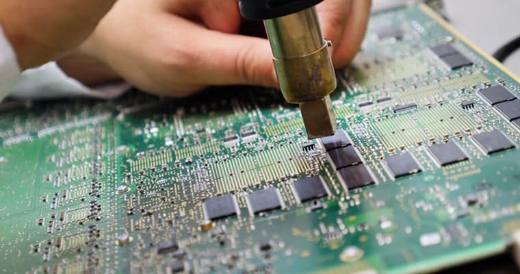
Typical HDI Fabrication Process
-
Material Preparation: Thin cores and prepregs are selected based on stack-up and thermal needs.
-
Lamination (Sequential Build-Up): Alternate thin copper foil and dielectric layers are laminated and selectively laser-drilled for microvias.
-
Laser Drilling: Precision lasers create microvias with clean walls—critical for reliable plating.
-
Desmear and Metallization: Plasma or chemical treatments clean the via walls; then copper plating deposits conductive copper into vias.
-
Imaging & Etching: Fine-line photolithography prints traces; etching removes unwanted copper.
-
Soldermask & Surface Finish: Apply soldermask (or dry film for very fine pads) and finish (ENIG, immersion silver, HASL alternative, etc.).
-
Component Assembly & Testing: Once PCBs are populated, in-circuit tests (ICT), flying probe tests, and thorough inspections validate quality.
Design Guidelines for Manufacturable HDI PCBs
-
Minimize Via-in-Pad unless you have a process to handle copper fill and planarity.
-
Control Trace Width & Spacing: Follow manufacturer DFM capabilities (e.g., 3–4 mil trace/space or finer as needed).
-
Specify Microvia Dimensions: Communicate drill diameter, target capture depth, and whether microvias will be stacked or staggered.
-
Stack-up & Impedance Control: Provide detailed stack-up and target impedance values for controlled impedance routing.
-
Annular Ring Considerations: Keep annular ring rules clear for reliability on microvias and blind vias.
-
Thermal Relief and Power Planes: Design power planes and thermal reliefs to avoid hot spots and improve solderability.
Working early with your PCB fabricator ensures your design aligns with their process windows and avoids re-spins.
Reliability, Testing & Quality Control
HDI boards require meticulous QA:
-
Cross-section analysis: Verifies via fill, plating thickness, and layer adhesion.
-
Automated Optical Inspection (AOI): Catches surface defects and fine-line anomalies.
-
X-ray Inspection: Essential for inspecting internal microvias and BGA solder joints.
-
Electrical Testing: ICT and flying probe tests verify continuity and absence of shorts.
-
Thermal and Stress Testing: DUTs may undergo thermal cycling, humidity testing, and vibration testing depending on the application.
A robust test plan reduces field failures and ensures long-term reliability.
Cost Considerations
HDI PCBs typically cost more per board than standard PCBs due to:
-
Advanced materials and thin cores
-
Laser drilling and finer photolithography equipment
-
More complex production steps (SBU, microvia formation, via filling)
-
Higher inspection and testing demands
However, HDI can reduce system-level costs by enabling smaller enclosures, fewer connectors, and better performance—often justifying the board-level premium.
Applications of HDI PCBs
-
Smartphones, tablets, and wearables
-
Medical devices (implantable and portable equipment)
-
Aerospace and defense electronics
-
High-performance computing and networking gear
-
Automotive advanced driver-assistance systems (ADAS) and sensors
How to Choose an HDI PCB Manufacturer
-
Check capabilities: Ask for minimum trace/space, microvia size, and max layer count for SBU.
-
Review qualifications: ISO, IPC compliance, experience with similar products.
-
Sampling & Prototyping: Start with a small prototype run to validate process and DFM limits.
-
Communication & Support: Fabricator should provide clear DFM guidance and quick turn feedback.
FAQs
Q1: What does HDI stand for?
A: HDI stands for High-Density Interconnect.
Q2: How small can microvias be?
A: Modern laser drilling can create microvias down to ~50 µm (0.05 mm) diameter, but typical production sizes range from 75–150 µm depending on the fab.
Q3: Are HDI PCBs more reliable than standard PCBs?
A: HDI PCBs can be equally or more reliable if manufactured and tested correctly. Reliability depends on design choices, via filling, material selection, and quality control.
Q4: Can I use HDI for RF or high-speed digital designs?
A: Yes — HDI benefits high-speed and RF designs by reducing trace lengths and improving signal integrity, but select appropriate high-frequency laminates if necessary.
Q5: Is via-in-pad recommended in HDI designs?
A: Via-in-pad is risky unless the via is plated and filled, and the fabricator can guarantee planarity. It is commonly used for BGA escape but requires controlled processes.
Q6: How does HDI affect lead times?
A: HDI may increase lead times due to additional process steps; however, many fabs now support fast-turn HDI if required (expect a premium).
Conclusion
HDI PCB manufacturing is essential for any product that demands compact size, high performance, and dense interconnects. While HDI brings additional material, process, and testing complexity, it unlocks critical advantages in miniaturization, signal integrity, and functional density. Successful HDI projects depend on early collaboration with your fabricator, clear stack-up and DFM specifications, and a thorough testing regime. With the right design practices and manufacturing partner, HDI PCBs can dramatically improve the performance and competitiveness of your electronic product.

