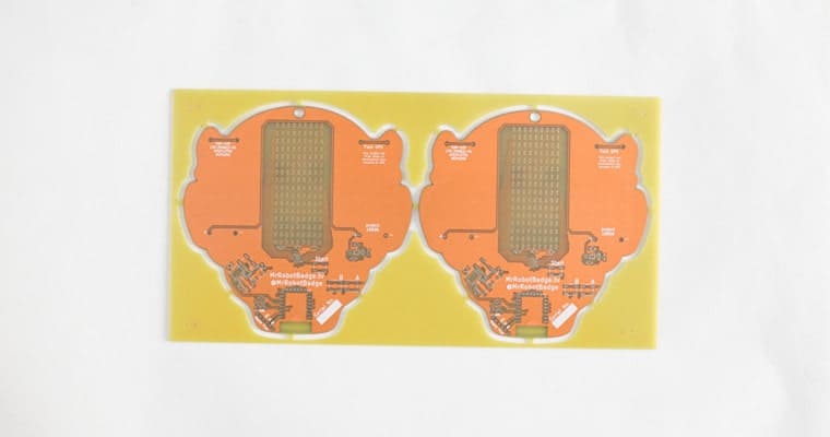
PCB thickness is one of the main factors that affect the performance of a Printed Circuit Board (PCB). In fact, it affects both the conductivity and resistance level of a PCB.
Table of Contents
ToggleThere is no official standard PCB thickness; there are particular sizes that manufacturers prefer. Thickness is altered for specific design purposes. Thus, manufacturers will ask you to choose between standard and minimum PCB thickness, depending on your design.
A preferred thickness size cuts down costs, leverages manufacturing equipment, and simplifies the overall PCB design.
PCB Thickness Options
1. Standard PCB Thickness
Most PCB manufacturers recommend 1.57mm (0.062 inches) as the standard PCB thickness size. This is the thickness that was used for manufactured bakelite sheets in the early days of PCB fabrication.
However, they still offer standard thickness in; 0.4 mm (0.016 inch), 0.5 mm (0.020 inch), 0.6 mm (0.024 inch), 0.8 mm (0.032 inch), 1.0 mm (0.04 inch), 1.2 mm (0.047 inch), 1.5 mm (0.062 inch), 1.6 mm (0.063 inch), 2.0 mm (0.079 inch), 2.3 mm (0.091 inch), and 3.175 mm (0.125 inch). Ultimately, the right thickness depends on your specific PCB project.
For instance, PCB projects with less demanding requirements call for a standard PCB thickness of 1.66mm (0.063 inches). This thickness will still offer maximum efficiency in terms of overall cost and leads time.
There are cases where the standard core thickness and solder mask coating are considered for controlled dielectric applications and controlled impedance. Thus, the effects of the solder mask must be considered as the solder mask decreases the impedance caused by thin traces.
2. PCB Copper Thickness
Copper plays a vital role in the overall thickness of a printed circuit board. It also dictates a PCB’s functionality. In fact, PCB copper thickness plays an essential role in achieving standard PCB thickness.
PCB copper thickness is achieved by spreading an ounce of copper evenly over a square foot area, which results in 1.37 mils (1.37 thousandths of an inch). Usually, all PCBs are manufactured with one ounce (10z) of copper.
The manufacturer presumes this as the right thickness for PCB applications across the board, even when the designer does not specify it. However, if the currents passing through the PCB application require the manufacturer to add the copper’s weight or the width of the trace, the total cost will increase because of the extra copper and the extended processing timeframe. The average copper thickness is 1.4mm to 2.8mm for internal layers and 2mm for the external layers. Copper thickness can be adjusted according to your requirements.
3. PCB Trace Thickness
PCB trace thickness is an essential parameter in PCB designs, and it is often determined by the manufacturer. It is specified in the designer’s Garber files to prevent damage or overheating. Usually, when the current flow increases, then copper traces heat up, causing a rise in temperature in the PCB.
On the flip side, if the temperature exceeds the limit of the PCB, then it is damaged. Thus, during the design process, the patch should be thick enough to allow current passage without affecting the average PCB temperature. This is where trace thickness comes in!
The trace should be thick enough to protect against the high current because current flow causes copper traces to overheat. This can damage the PCB. As the task of calculating trace would be cumbersome, designers opt to use a trace width calculator to determine appropriate trace thickness.
4. Custom Thickness
PCBs are available in readymade sheets and sizes. More often than not, your manufacturer has the PCB of your preferred thickness in stock or can quickly obtain it. But did you know that you can specify your PCB thickness?
The thickness ranges from 0.2mm to 6.3mm in hundredths of millimeter increments. Yes, you read that right! There are two-layer PCBs that are as thin as 0.2mm! As PCB thickness options appear on the specification tab of your designer’s PCB workspace, all you have to do is select the custom thickness option.
This prevents your design from being panelized by other designs. Therefore, minimum PCB area charges will apply. When creating custom thickness, the PCB fab starts with a set of common core and prepreg thicknesses, then combines them in the necessary sequence, along with copper foil, solder mask, and copper plating thickness to reach the desired final thickness.
However, custom thickness is only specific to your PCB, and it will be designed only for you. By stating your thickness preference, your manufacturer will let you know whether the design is possible.
How To Specify PCB Thickness
You should be able to specify your PCB thickness after considering these factors:
1. Manufacturer’s Equipment Capability
This is the first and most important consideration for your PCB thickness. If the manufacturer does not have the equipment to produce a certain type of thickness, they will not meet your design requirements.
They may not be able to manufacture the printed circuit board altogether. Determine this in the early stages of the manufacturing process. If not, you will be forced to make modifications to your PCB layout.
2. Size and Weight
Thinner PCB boards are lighter. This means that they are more flexible than their thicker counterparts. Despite their flexibility, thin boards are brittle.
If your application does not require flexibility, then you can use a considerable amount of thickness. This will offer strong structural integrity.
Thicker boards also come with a downside, including the consumption of a lot of space within a device. This may pose a problem for an application with limited space capacity. The size and weight are the first parameters that define the PCB design.
3. Board Materials
The lifetime of a PCB board and its operation depends on the choice of materials. Typical board fabrication consists of the substrate, laminate, solder mask, and silkscreen. Even so, the substrate and laminate are the most important for consideration.
The substrate often consists of a glass weave, epoxy, or paper resin, depending on the dielectric constant. On the other hand, laminates consist of cloths or paper layers. These materials not only affect the structure of the board but also the overall thickness.
4. Types of Signals
PCB boards carry multiple signals. These signals determine the materials that are used in the manufacturing process, and they choose the ultimate thickness of the board.
For instance, if your PCB board carries high power signals, it will require thick, copper-wide traces. This means that the board will be significantly thicker.
5. Number of PCB Layers
The more layers your PCB board requires, the thicker it will be. While two to six layers will offer standard PCB thickness, eight or more layers will not. Manufacturers may use thinner PCBs to achieve standard thickness, making it increasingly impractical as the layers increase.
If you are looking for standard thickness, cutting down on your PCB layers is paramount. However, if your design needs more layers, then you will have to allow greater thickness.
6. Operating Environment
The thickness of the board and the materials that are used in the design process affects your PCB’s conductivity.
A PCB board with thin thickness will not thrive in a rugged operating environment as this requires a thick and sturdy PCB.
On the flip side, PCB boards that come with thick copper traces are sub-optimal for high-voltage environments. By considering such factors, manufacturers can determine the desired thickness level.
Going over all of these factors with your manufacturer is important as it will guide the design and production process. It will equally give your manufacturer the capability to express their abilities.
There are instances when manufacturers determine the best thickness for an application, while others will advise on customization. Here is how to specify your PCB thickness option:
1. The Turnaround Time
Standard PCB thickness options are common and require minimal adjustments. On the other hand, custom thickness requires a change to the manufacturer’s equipment and work processes to accommodate unique design needs.
Some adjustments may take time and delay the design and manufacture process. This will have an impact on the turnaround time.
It is advisable to discuss the delivery time estimates with your manufacturer once you choose PCB thickness.
2. Additional Costs
It would be best if you discussed any additional costs with your manufacturer. Remember, a custom board will offer cost-effective benefits for your business.
However, they come with additional costs due to the delayed manufacturing process. When considering costs, you should closely assess the cost versus the benefits that your business will enjoy.
Final Thoughts
PCB thickness determines PCB functionality. Therefore, you should be confident that your manufacturer will consider all of the elements mentioned above for optimum results. But remember, PCB thickness is not a “one-size-fits-all” option. Depending on your business needs and application, it may be easy to go with the standard thickness options or customize if you are looking for uniqueness.
There are several PCB thickness options available apart from what people refer to as ‘standard measurements.’ Though using a standard PCB thickness results in faster and cost-effective manufacturing, custom thicknesses ensure you obtain the right functionality for your custom application. Regardless of your choice, you should partner with a reputable and professional PCB manufacturer that can meet your needs and provide professional advice.
MKTPCB is a PCB manufacturer based in Shenzhen, China. As the leading manufacturer and supplier of PCBs, we strive to give our clients the best products throughout the year. Are you interested to learn more about our PCB assembling capacities? Do you need professional advice regarding various PCB thickness options? Contact us today to get answers to all your questions.


