

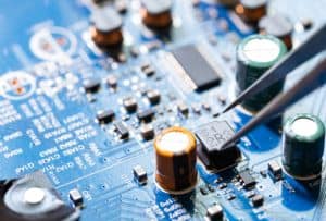


Circuit traces are the backbone of printed circuit boards (PCBs).
They form the conductive pathways that link components and enable electrical signals to flow reliably.
Understanding how traces work, the materials used, and their design parameters is crucial for creating durable and high-performance PCBs.
This guide explains the fundamentals of circuit traces, offers practical design tips, and highlights best practices for avoiding common problems.
What Are Circuit Traces?
Circuit traces are thin conductive paths etched or printed onto PCB substrates.
They replace traditional wiring by embedding connections directly into the board’s layers, saving space and improving reliability.

Traces come in different widths, thicknesses, and shapes depending on current requirements and signal speeds.
They are typically made of copper because of its excellent conductivity and cost-effectiveness.
Well-designed traces ensure minimal resistance and reduce the chance of signal loss or overheating during operation.
Understanding the basic structure of a circuit trace lays the foundation for effective PCB design.
Definition and Role of Circuit Traces
A circuit trace acts as a wire embedded in the board.
It carries electrical signals or power between components, forming the functional network of the circuit.
Trace layout affects performance, noise levels, and thermal behavior.
Even small design changes, such as altering the width or routing, can impact current capacity or impedance.
Designers treat traces as both electrical and thermal conductors, balancing size with performance and space constraints.
Common Materials Used in PCB Traces
Copper is the standard choice for PCB traces due to its high conductivity and affordability.
For specialized applications, gold, silver, or aluminum coatings may be applied to reduce corrosion or improve solderability.
The substrate beneath, often FR-4 fiberglass, also influences thermal and electrical performance.
Material selection depends on factors like cost, required current, and environmental conditions.
Using high-quality materials ensures better long-term reliability and reduces the likelihood of maintenance issues.
Key Design Considerations for Circuit Traces
Designing effective circuit traces requires balancing electrical, thermal, and physical constraints.
Trace width and thickness determine how much current it can safely carry.
Routing must minimize sharp angles to reduce stress points and signal reflections.
Thermal management, via thicker copper layers or heat sinks, prevents overheating.
Good design practices improve performance and extend the lifespan of the PCB.
Trace Width and Thickness
Trace width directly affects resistance and heat buildup.
Wider traces can carry more current and dissipate heat better.
Designers use standard calculators or IPC-2221 guidelines to select optimal dimensions.
Thickness, often expressed in ounces of copper per square foot (e.g., 1 oz/ft²), also affects capacity.
Combining correct width and thickness ensures safe operation and efficient performance.
Current Capacity and Thermal Management
Current capacity is the maximum current a trace can carry without overheating.
When currents rise, traces heat up, risking delamination or failure.
Thermal management strategies include thicker copper, thermal vias, or dedicated ground planes.
Maintaining safe temperatures protects both the trace and the components it connects.
This approach is essential for power electronics or high-density designs.
Advanced Practices for High-Performance Circuit Traces
As circuits get faster and more compact, trace design becomes critical for maintaining signal integrity.
Advanced practices like impedance control, controlled routing, and noise reduction help achieve consistent performance.
Designers must also consider electromagnetic interference (EMI) and cross-coupling between adjacent traces.
Applying these techniques ensures reliable operation in high-speed or high-frequency applications.
Impedance Control in High-Speed Circuits
Impedance is the opposition a trace presents to alternating current.
Maintaining consistent impedance prevents signal reflections and data errors.
Controlled impedance traces are designed by adjusting width, thickness, and dielectric spacing.
Tools like field solvers or PCB design software help calculate and maintain these parameters.
This practice is crucial for RF circuits, high-speed data buses, and sensitive analog paths.
Minimizing Crosstalk and Signal Loss
Crosstalk occurs when signals in adjacent traces interfere with each other.
To minimize it, designers maintain proper spacing, use ground planes, and route signals perpendicularly between layers.
Reducing sharp bends and maintaining equal trace lengths also improves signal quality.
These strategies cut signal loss and ensure accurate data transmission.
Common Issues and How to Prevent Them
Poorly designed traces can cause overheating, mechanical failure, or signal problems.
Recognizing common issues helps designers take preventive steps early.
Selecting the right materials, dimensions, and routing rules is essential.
Testing prototypes under expected loads verifies that traces will perform reliably in the field.
Overheating and Delamination
Overheating damages traces by softening adhesives or causing copper to lift from the substrate.
Delamination weakens the PCB and may lead to open circuits.
Preventing this requires proper trace sizing, heat dissipation features, and conservative current ratings.
Monitoring temperature during testing also identifies weak points before production.
Corrosion and Reliability Concerns
Environmental exposure, such as moisture or chemicals, can corrode copper traces.
Protective coatings like solder masks or conformal coatings shield traces from damage.
Gold or silver plating further improves oxidation resistance.
Implementing these measures extends PCB life and reduces maintenance needs.
(FAQs)
Q1: How do I calculate the correct trace width for my PCB?
Use IPC-2221 standards or online calculators based on current, copper thickness, and temperature rise.
Q2: What materials are best for circuit traces in harsh environments?
Copper with protective coatings like gold or conformal coatings is recommended for corrosion resistance.
Q3: How can I improve signal integrity in high-speed circuits?
Control impedance, maintain spacing between traces, and use ground planes to reduce interference.
Q4: Why do PCB traces overheat?
They overheat when the current exceeds their capacity or when thermal management is inadequate.
Q5: What’s the difference between internal and external PCB traces?
External traces are exposed on the surface, while internal traces are embedded within PCB layers for protection and controlled impedance.

